In semiconductor fabs, R&D labs, and optical coating facilities, knowing the exact thickness and optical properties of thin films is critical – yet traditional contact methods can damage delicate samples or miss crucial data. Today, MSK (Tianjin) International Trading CO.,Ltd. announces its latest spectroscopic ellipsometer, a non‑destructive thickness measuring instrument engineered for wafer thickness measurement, refractive index analysis, and multi‑layer stack characterization.
This new system combines a broad spectral range, high sensitivity, and user‑friendly modeling software – all in a compact, research‑grade platform. Whether you need to measure ultra‑thin gate oxides, anti‑reflection coatings on solar cells, or complex OLED stacks, MSK’s spectroscopic ellipsometer delivers reliable, repeatable data without contacting or damaging your sample.
“Engineers often struggle to balance precision, speed, and sample safety,” said a senior MSK product manager. “Our spectroscopic ellipsometer solves that – as a true thickness measuring instrument, it provides wafer thickness measurement and optical constant analysis in seconds, with zero risk of scratching or contamination.”
Why Choose This Spectroscopic Ellipsometer as Your Thickness Measuring Instrument
Unlike single‑wavelength or mechanical profilers, this spectroscopic ellipsometer uses polarized light to analyze how a thin film modifies the light’s polarization state. From that measurement, it calculates multiple parameters simultaneously:
- Film thickness (single‑layer to complex multi‑layer stacks)
- Refractive index (n) and extinction coefficient (k)
- Optical band gap (Eg)
- Surface roughness
As a versatile thickness measuring instrument, it handles thicknesses from ultra‑thin (sub‑nanometer) to relatively thick films – making it suitable for everything from atomic layer deposition to micron‑scale polymer coatings.
Non‑Destructive Wafer Thickness Measurement – Critical for Semiconductor Production
For semiconductor manufacturing, wafer thickness measurement is essential to control deposition, etching, and CMP processes. However, mechanical stylus profilers can scratch soft films, and optical reflectometers often lack sensitivity for multi‑layer stacks.
MSK’s spectroscopic ellipsometer overcomes these limitations:
- Non‑contact & non‑destructive – no risk of damage to patterned wafers or delicate films
- High sensitivity – capable of detecting sub‑nanometer thickness variations across the wafer
- Multi‑layer analysis – measures individual layers in complex stacks (e.g., SiO₂/Si₃N₄/poly‑Si) without cross‑talk
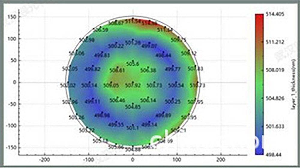
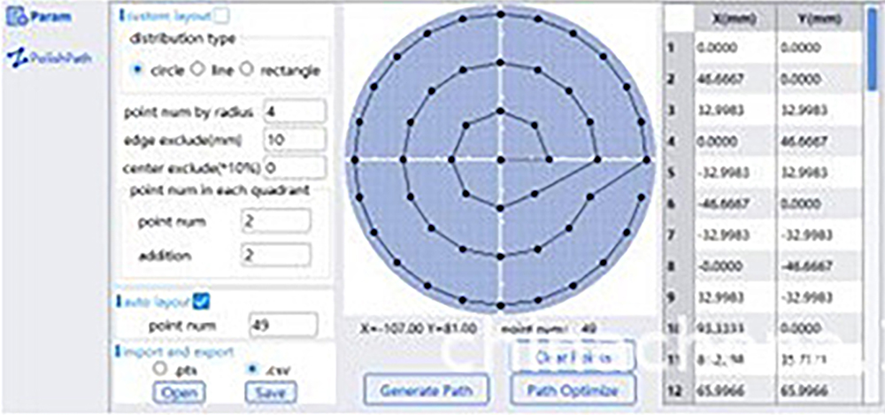
The system includes an automatic mapping stage that supports wafers up to 8 inches (200mm) with precise positioning. Users can generate 2D and 3D thickness distribution maps with a single click – ideal for process uniformity monitoring.
Beyond Semiconductors: Wide Application Range
While optimized for wafer thickness measurement, this spectroscopic ellipsometer serves many industries:
- Flat panel displays – measure OLED and TFT layer thicknesses
- Photovoltaics – characterize anti‑reflection coatings, transparent conductive oxides, and absorber layers
- Optical coatings – verify bandpass filters, anti‑reflection stacks, and high‑reflectivity mirrors
- Materials science – study thin films, 2D materials, and polymers
- Bio‑sensing – detect molecular layers on functionalized surfaces
The instrument’s wide spectral range (from ultraviolet to near‑infrared) allows it to characterize materials from deep‑UV lithography films to infrared optical coatings.
Advanced Yet Easy‑to‑Use: Software That Works for You
A powerful thickness measuring instrument must also be practical for daily use. MSK’s spectroscopic ellipsometer comes with comprehensive analysis software that features:
- Pre‑built optical constant database – over 100 materials including common semiconductors, dielectrics, and metals
- Multiple dispersion models – Cauchy, Sellmeier, Tauc‑Lorentz, B‑spline, oscillators, and more
- Multi‑layer fitting – supports up to 30 layers, including graded interfaces and surface roughness
- One‑click mapping – automatically generates thickness uniformity reports for wafers and large substrates
- Offline licensing – allows data analysis on separate computers without tying up the instrument
The guided, interactive interface reduces training time – new users can perform routine wafer thickness measurement within minutes.
Designed for Research & Production Environments
MSK offers this spectroscopic ellipsometer in multiple configurations to match your needs:
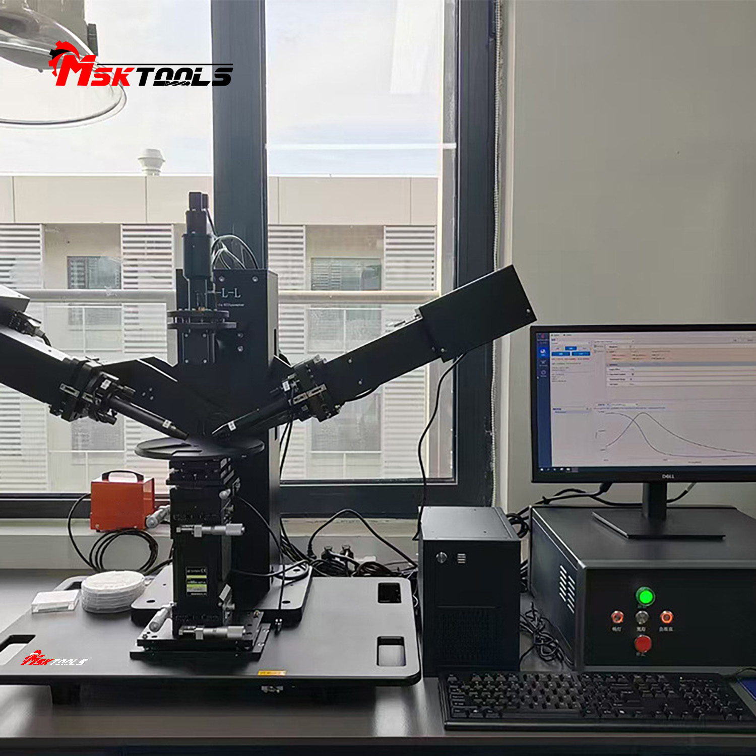
- Benchtop system – perfect for R&D labs and university research
- Mapping configuration – includes high‑precision X/Y stage for automated wafer scanning
- Customizable spectral ranges – from deep UV (193nm) to short‑wave infrared (2500nm)
- Temperature‑controlled stage options – for in‑situ measurements up to 1000°C
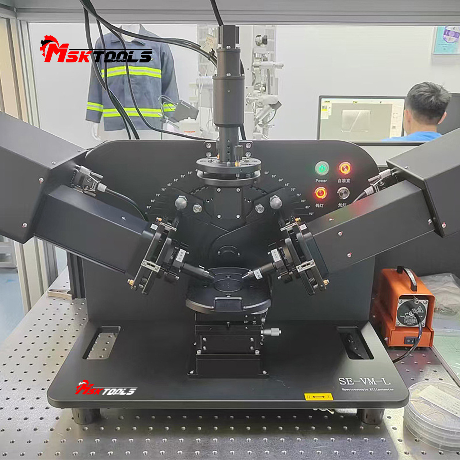
The instrument uses dual‑rotating compensator technology, which measures all 16 Mueller matrix elements in a single acquisition. This provides richer data than conventional ellipsometers – especially useful for anisotropic or depolarizing samples.
Reliable Performance for Critical QC
For production environments, repeatability is everything. MSK’s spectroscopic ellipsometer delivers exceptional stability thanks to:
- Semiconductor‑cooled detectors – low noise, high dynamic range
- Laser auto‑focus – maintains consistent focal position across the sample
- Stable optical path design – minimizes drift between calibrations
The system meets rigorous industry standards, and MSK provides third‑party metrology reports to verify absolute thickness accuracy on standard samples.
Customization & Support – Tailored to Your Application
MSK understands that every thin film application is unique. That’s why the company offers:
- Custom spectral range extensions – choose the bands that match your materials
- Specialized sample stages – for non‑standard wafer sizes or oddly shaped substrates
- Software customization – add specific analysis models or automation routines
- On‑site installation & training – get your team up to speed quickly
Because this is a high‑precision instrument, the price shown on the product page is a deposit only. MSK invites serious buyers to contact the sales team for an exact quote based on your required configuration.
Free Technical Consultation & Demo
Not sure if ellipsometry is right for your material? MSK offers complimentary technical consultation.
Availability & Contact Information
The new spectroscopic ellipsometer series is available immediately for global orders. To request a quote, receive a product brochure, or arrange a live online demo:
Email: molly@mskcnctools.com
Phone: 0086-13602071763
Web: www.mskcnctools.com
MSK welcomes inquiries from semiconductor fabs, research institutes, optical coating manufacturers, and solar cell producers – from single units to multiple systems.
About MSK CNC Tools
Founded in 2015 and ISO 9001 certified, MSK (Tianjin) Cutting Technology Co., Ltd. specializes in high‑precision metrology instruments and CNC cutting tools. With German and Taiwanese manufacturing equipment and a dedicated R&D team, MSK serves customers across Europe, America, and Asia. The company’s mission is to provide advanced, reliable, and cost‑effective solutions for material characterization and machining.
Post time: Apr-10-2026


