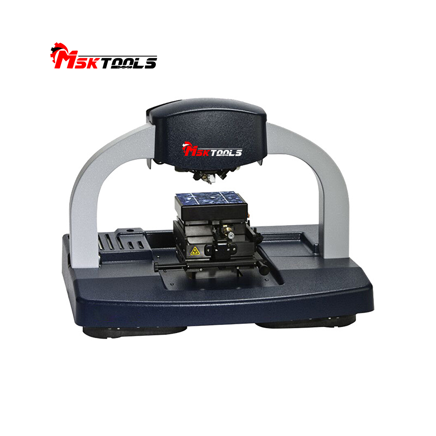
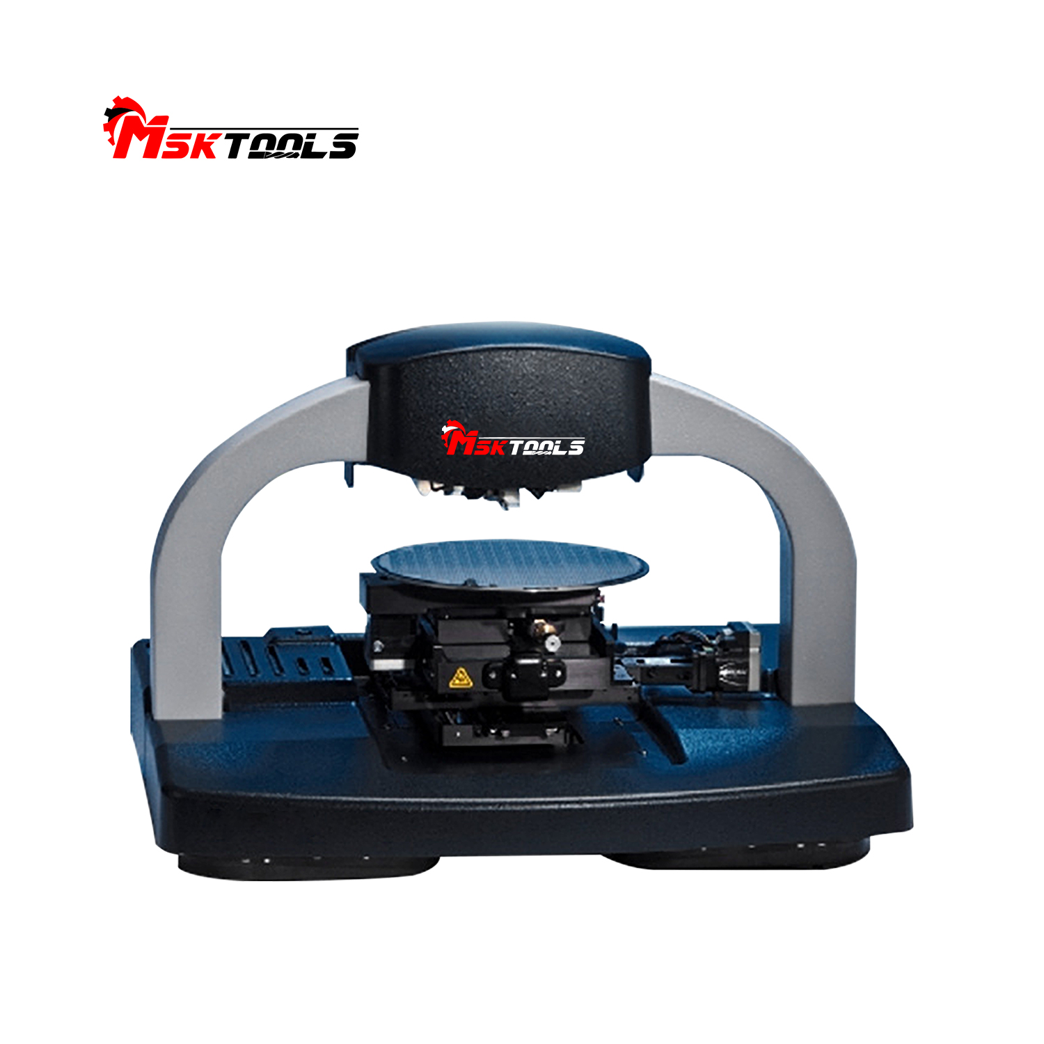
High Precision Stylus Surface Profiler | Nanometer Step Instrument for Semiconductors


Ordering Instructions
Due to the special nature of the product, the price shown on the page is a deposit price, not the actual price. Please contact customer service for a quote.
Orders placed directly without prior contact cannot be shipped! Thank you for your cooperation! For more product information, please contact customer service to receive product brochures.
High Precision Stylus Surface Profiler – Nanometer Step Height & Surface Roughness Measurement
This contact‑type stylus surface profiler is a precision metrology instrument designed for high‑resolution measurement of step height, surface roughness, and 3D topography. Using a diamond stylus that gently scans the sample surface, the system accurately tracks microscopic peaks and valleys to deliver reliable, repeatable data for quality control, R&D, and production environments.
How It Works
The measurement principle is based on a stylus‑based contact method. As the stylus moves across the surface, its vertical displacement follows the surface profile. This movement is converted into an electrical signal via a measuring bridge, producing an amplitude‑modulated output proportional to the displacement. After amplification, phase‑sensitive rectification, and advanced filtering (including noise and waviness filters), the system outputs a clean, stable signal—free from external interference and waviness effects—ensuring high‑accuracy roughness and step height analysis.
Key Applications
Semiconductor wafer metrology
MEMS and microstructures
Thin film and coating thickness
Solar cell surface profiling
Precision optics and medical devices
Product Advantages:
Stable performance, fast transmission, automatic calibration, accurate measurement, rapid response, and real-time monitoring.
Stable performance, desktop design.
The revolutionary desktop design achieves a balance of high performance, ease of use, and cost-effectiveness.
Compact and reliable design
Optimized hardware configuration, compact structure, improved testing accuracy and stability, and high efficiency.
Superior materials, durable and long-lasting.
Exquisite workmanship, craftsmanship, high efficiency, and long service life.
Product Information
Product Overview: The Step instrument Probe Profilometer (Step Analyzer) features a revolutionary benchtop design, combining industry-leading technology and design to achieve a balance of high performance, ease of use, and cost-effectiveness, with improved process control from R&D to quality control.
The device achieves excellent repeatability at 4A (0.4nm) and a 40% increase in scanning speed, supporting nanoscale surface topography measurement technology in industries such as microelectronics, semiconductors, touchscreens, solar energy, high-brightness LEDs, medical, and materials science.
Equipment Features
Unrivaled Performance, Step Height Reproducibility Below 4A
Innovative design, comprehensive accessories, and optimized operating and analysis software enable Step instrument to achieve enhanced performance and superior step height reproducibility.
Single-arch Design for Breakthrough Scan Stability
The single-arch design makes Step instrument more robust, minimizing the impact of ambient noise. Step instrument's scanning probes enable simultaneous large vertical range and low-force scanning.
Upgraded "Smart Electronics" for Improved Measurement Accuracy and Stability
Step instrument's upgraded "Smart Electronics," employing an advanced processor, reduces noise levels, making it a more powerful system capable of measuring step heights <10nm.
Optimized Hardware Configuration Reduces Data Acquisition Time by 40%
Utilizing a unique direct-drive scanning stage, measurement time is accelerated by 40% while maintaining industry-leading performance. Step instrument's 64-bit parallel processing Vision64 completes and processes large 3D data files in less time.
64-bit Vision64 synchronous data processing software increases data analysis speed tenfold.
Vision64 is Step instrument's 64-bit parallel processing operation and analysis software, enabling faster loading of 3D topography data and faster application of filters and multi-region database analysis.
Intuitive Vision64 user interface for easier use.
Vision64 software provides an intuitive and simplified user interface, combining intelligent architecture and customizable automation functions for rapid and comprehensive data collection and analysis. Step Instruments' Vision64 significantly simplifies and accelerates operation and data analysis.
Automatic Tip Alignment System for Easy Probe Changes
Step instrument's self-aligning probe assembly allows users to quickly and easily change between different probes, eliminating potential risks during the changeover process.
Wide Range of Probe Models
Step instrument offers a wide range of probe sizes and shapes to meet virtually every application need. Step instrument features a faster and simpler probe changeover process.
Single Sensor Design
Provides low force and a wide scan range on a single plane.
Ensuring High Throughput Testing
Step instrument enables quick and easy setup and execution of automated multi-sample measurement modes to verify the precise thickness of thin films across the entire wafer surface with superior repeatability. This effective monitoring saves valuable time and money by increasing test throughput.
Application Cases
Thin Film Testing - Ensuring High Yields
In semiconductor manufacturing, rigorous monitoring of deposition and etching ratio uniformity, thin film stress, and ITO thin film thickness measurement on touchscreen panels can save significant time and money. Inhomogeneity or excessive stress in the thin film can lead to low yields and poor finished product performance. Step instrument allows for easy and quick setup and execution of automated multi-point testing programs to verify the precise thickness of wafer thin films down to the nanometer level. Step instrument's strong reproducibility provides engineers with accurate thin film thickness and stress testing to precisely adjust etching and deposition for optimal results.
Surface Roughness Inspection - Ensuring Performance
Step instrument is suitable for routine surface roughness assessment of precision machine parts in many industries, including automotive, aerospace, and medical devices. For example, the roughness of the hydroxyapatite coating on the back of orthopedic implants can affect post-implant adhesion and efficacy. Rapid surface roughness analysis using Step instrument can determine whether crystal production meets expectations and whether implants meet product requirements. Using the Vision64 database's pass/fail criteria, quality management departments can easily determine whether implants need to be reworked or their quality ensured.
Solar Grid Line Analysis - Reducing Manufacturing Costs
In the solar market, Step instrument is ideal for measuring the critical dimensions of conductive silver grid lines on monocrystalline and polycrystalline silicon solar panels. The height, width, and continuity of the silver lines are closely related to the energy conduction of the solar cell. Ideally, production should utilize silver appropriately to achieve better conductivity without wasting expensive silver. Step instrument achieves this through software analysis, reporting the critical dimensions of the silver grid lines to determine the precise components required for conductivity. Vision64's data analysis methods and automation features contribute to automating this verification process.
Microfluidics Technology - Detecting Design and Performance
Step instrument is a probe profilometer capable of measuring photosensitive materials with angstrom-level reproducibility over a large vertical range (up to 1 mm). Researchers in the MEMS and microfluidics technology industries can use Step instrument for qualification testing to ensure parts meet specifications. The low-force measurement function NLite+ lightly touches the photosensitive material to measure vertical steps and roughness.
Technical parameters
| Measurement Technology | Probe profiling technology |
| Measurement Function | 2D surface profile measurement |
| Optional 3D measurement/ | |
| Sample View | Selectable magnification, 1 to 4mm FOV |
| Probe Sensor | Low inertia sensor (LIS3) |
| Probe Pressure | Using LIS3 sensor: 1 to 15mg |
| Low Force (Optional) | Using N-Lite+ low force sensor: 0.03 to 15mg |
| Probe Options | Probe curvature radius selectable range: 50nm to 25μm; |
| Height-to-diameter ratio (HAR) tips: 10μm*2μm and 200μm*20μm; | |
| Custom tips are available upon request. | |
| Sample X/Y Stage | Manual X-Y translation: 100mm (4 inches) |
| Motorized X-Y translation: 150mm (6 inches) | |
| Sample Rotary Stage | Manual, 360° rotation; |
| Motorized: 360° rotation; | |
| Computer System | 64-bit multi-core line processor, Windows* 7.0; Optional 23-inch flat panel display |
| Software | Vision64 operation and analysis software; |
| Stress measurement software: Cantilever deflection; | |
| Suturing software: 3D scanning imaging software | |
| Vibration Damping Device | Shock damping available |
| Scan Length Range | 55mm (2 inches) |
| Data points per scan | Up to 120,000 data points |
| Maximum sample thickness | 50mm (2 inches) |
| Maximum wafer size | 200mm (8 inches) |
| Step height reproducibility | <4A1σ on a 1μm step |
| Vertical Range | 1mm (0.039 inches) |
| Vertical Resolution | Maximum 1A (at 6.55μm vertical range) |
| Input Voltage | 100 - 240 VAC, 50 - 60Hz |
| Temperature Range | Operating Range 20 to 25°C (68 to 77°F) |
| Humidity Range | ≤80%, Non-condensing |
| System size and weight | 455mm W x 550mm D x 370mm H |
| (179in. W x 22.6in. D x 14.5in. H); | |
| 34 kg (75 lbs); | |
| Attachment: 550mm L x 585mm W x 445mm H (216in. L x 23in. W x 175in. H); | |
| 217 kg (48 lbs) |
About Us
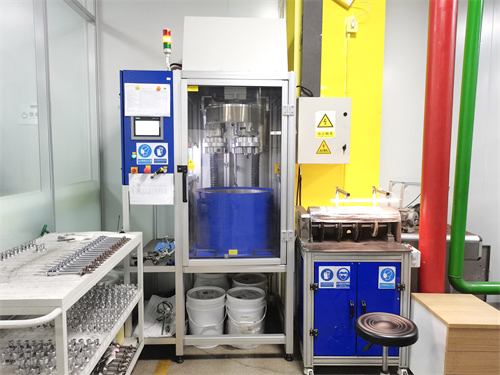
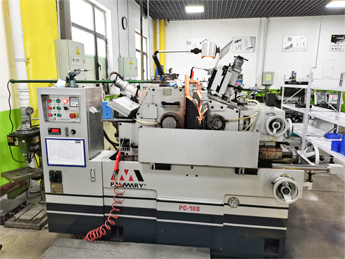
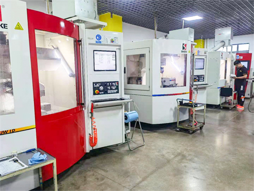
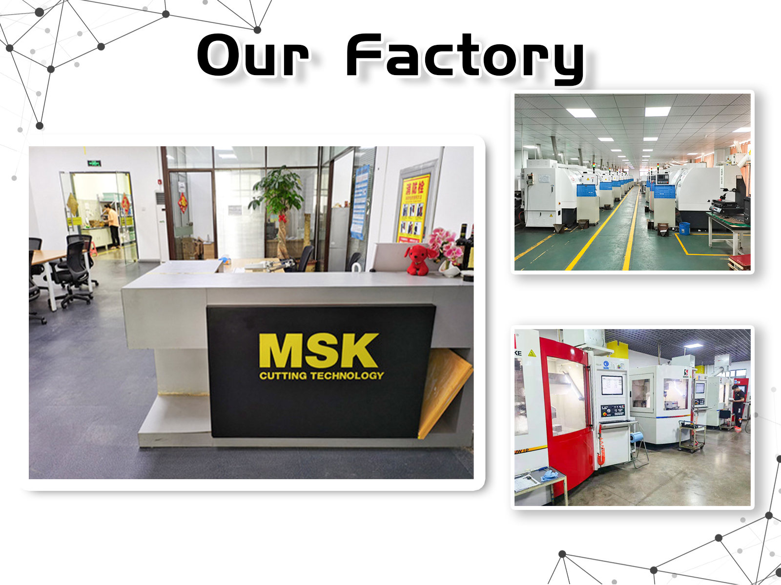
Factory Profile
Why Choose Us

FAQ
Q1: Who are we?
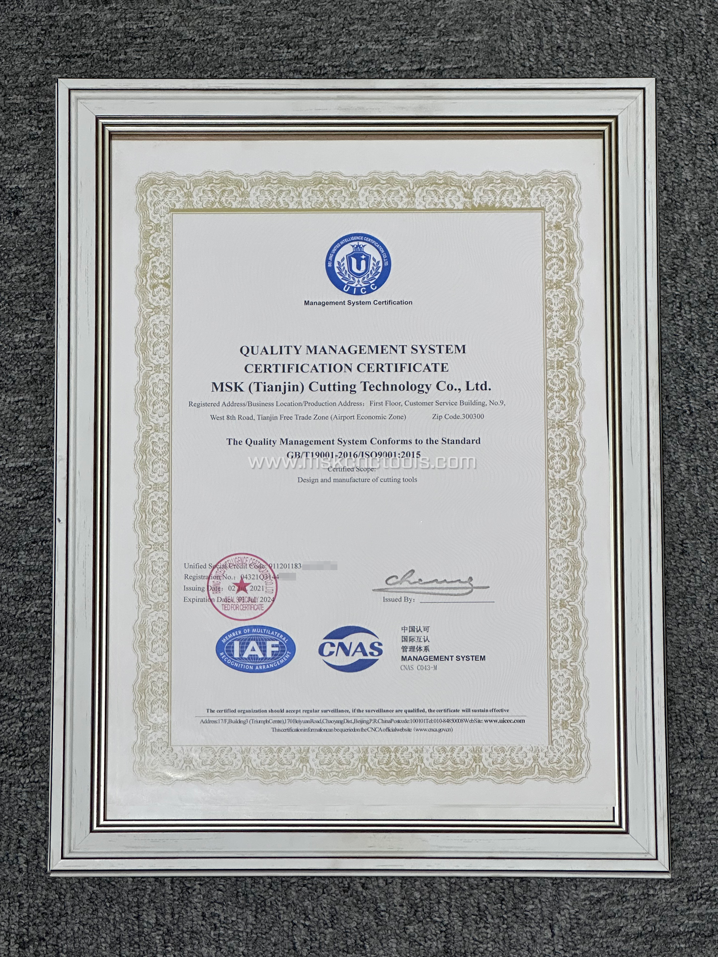
A1: Founded in 2015, MSK (Tianjin) Cutting Technology CO.Ltd has grown continuously and passed Rheinland ISO 9001
authentication.With German SACCKE high-end five-axis grinding centers, German ZOLLER six-axis tool inspection center, Taiwan PALMARY machine and other international advanced manufacturing equipment, we are committed to producing high-end,professional and efficient CNC tool.
Q2: Are you trading company or manufacturer?
A2: We are the factory of carbide tools.
Q3: Can you send products to our Forwarder in China?
A3: Yes,if you have Forwarder in China,we will glad to send products to him/her.
Q4: What terms of payment are acceptable?
A4: Normally we accept T/T.
Q5: Do you accept OEM orders?
A5: Yes, OEM and customization are available, and we also provide label printing service.
Q6: Why should you choose us?
A6:1) Cost control - purchasing high-quality products at an appropriate price.
2) Quick response - within 48 hours, professional personnel will provide you with a quote and address your concerns.
3) High quality - The company always proves with sincere intention that the products it provides are 100% high-quality.
4) After sales service and technical guidance - The company provides after-sales service and technical guidance according to customer requirements and needs.